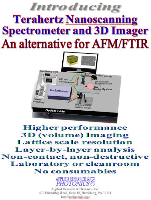
TNS3DI
What is Terahertz? Why Important?
Terahertz radiation – also known as submillimeter radiation, terahertz waves, tremendously high frequency (THF), T-rays, T-waves, T-light, T-lux or THz – consists of electromagnetic waves within the ITU-designated band of frequencies from 0.1 THz to 30 THz. One THz is 1012 Hz or 1000 GHz. Wavelengths of radiation in the terahertz band correspondingly range from 3 mm down to 0.01 mm (or 10 μm). Because terahertz radiation (T-ray) has a wavelength of millimeter and proceeds into shorter wavelengths, it is sometimes known as the submillimeter band, and its radiation as submillimeter waves, especially in astronomy. [1]
T-ray can penetrate thin layers of materials but is blocked by thicker objects. T-ray beams transmitted through materials can be used for material characterization, layer inspection, and as an alternative to X-ray for producing high resolution images of the interior of solid objects.
 |
| Figure 2 |
Why are terahertz frequencies useful?
- T-Ray energy too weak to knock of the electrons from atoms, thus, non-ionizing.
- Far less energy than X-rays; no bond-breaking, i.e. no radiation dose or damages.
- Higher resolution than other safe wavelengths; see notes on lattice resolution imaging with T-Ray.
- Most materials are transparent to T-ray; so, one can “see” under the surface without destruction
- T-Ray wavelength is suitable for probing biological molecules and tissue
Comments and Contact
Please email: info@arphotonics.net
Camera-less Lattice Resolution Imaging without Electron Microscope
The Next Generation Imaging Technology - Replacement for an Atomic Force Microscope
- Q: How to achieve Angstrom scale image resolution with bigger wavelength?
Combination of the three components produce Angstrom scale resolutionSee: Breaking the Abbe Diffraction Limit
See here for details: Nanoscale Metrology of Line Patterns on Semiconductor by Continuous Wave Terahertz Multispectral Reconstructive 3-D Imaging Overcoming the Abbe Diffraction Limit
Breaking the Abbe Diffraction Limit
This is the key to the camera-less lattice scale imaging without electron microscope. |
| Figure 3. |
“Abbe diffraction limit,” [1] sets the highest resolution achievable as half of the wavelength of the light used for imaging. This rule is the “bible” for imaging since 1873 as was set by Ernst Abbe [1].
Scientists have been trying to break this limitation over many decades. While achieving very high resolution by breaking the diffraction limit has been a focus for the modern optics [2], up until now there has not been much progress for characterizing a whole wafer, both on its surface and across the thickness, or the sub-surfaces, in a non-destructive, non-contact mode, with layer by layer inspection capability, except the route demonstrated in ref. [3]. Semiconductor manufacturing is a complicated process; as such a wafer must undergo a number of critical testing in the blank form, at various stages of process development, and at the final stage with patterned devices. The present work demonstrates an alternative that is less laborious and provides additional information than what is available from the current state-of-the-art.
The resolution of an optical-lens-based imaging system is defined by the Abbe paradigm (“ADL”) as d = l/(2n.Sina), where λ is the wavelength. For free-space, d ~ λ/2.
Since the wavelength of electrons is (2.5 pm at 200 keV), which is much smaller than that of photons, so, the resolution of an electron microscope (EM) is theoretically ~1.2 pm. In practice, the resolution of an EM is limited to ~0.1 nm due to the objective lens system.
Current techniques, such as SEM, TEM, AFM, STM, and FIB produce a frozen-in-time image of a single surface. They are destructive and suitable for small sample sizes. Requires high vacuum.
Q: how to break the Abbe diffraction limit?
[1] For details, see here: Nanoscale Metrology of Line Patterns on Semiconductor by Continuous Wave Terahertz Multispectral Reconstructive 3-D Imaging Overcoming the Abbe Diffraction Limit
Features, Benefits and Capabilities of TNS3DI
Terahertz Nanoscanning Spectrometer & 3D Imager (TNS3DI)The Applied Research & Photonics model TNS3DI – utilizing its proprietary Dendrimer Dipole Excitation technology to deliver what we have demonstrated is unsurpassed analytical, and imaging capability to enable the revolution in advanced materials and structures that are changing the world today. The system has demonstrated the ability to pinpoint and catalyze the deep investigation and understanding scientists and engineers all over the world have been searching for, to solve some of the most challenging problems in advanced materials, semiconductors and related devices, photonics and optoelectronics including displays, medical, biological and pharmaceutical applications, and atomic/nuclear level investigations.


Comments
Post a Comment